AI PCB Design: My AI Tried to Make Itself Physical [2026]

This morning, I asked my AI to design itself a body. In under an hour, the finished factory files were sitting in a folder on my screen — the complete, manufacture-ready design for a real circuit board, created almost entirely by an AI, printable for about the price of a coffee.
That sentence would have been science fiction eighteen months ago. AI PCB design — using AI to create real, physical electronics — has quietly crossed the line from research demo to something you can genuinely do this weekend, with no electronics lab and no experience.
In this guide, we'll look at what AI can actually do in hardware design (and what it still gets dangerously wrong), the three routes you can take from idea to physical board, and the full story of my own experiment — told partly by the AI itself. Let's start with the question everyone asks first.
Can AI Really Design a Circuit Board?
Yes — with supervision. And the fact that it can matters more than most people realise.
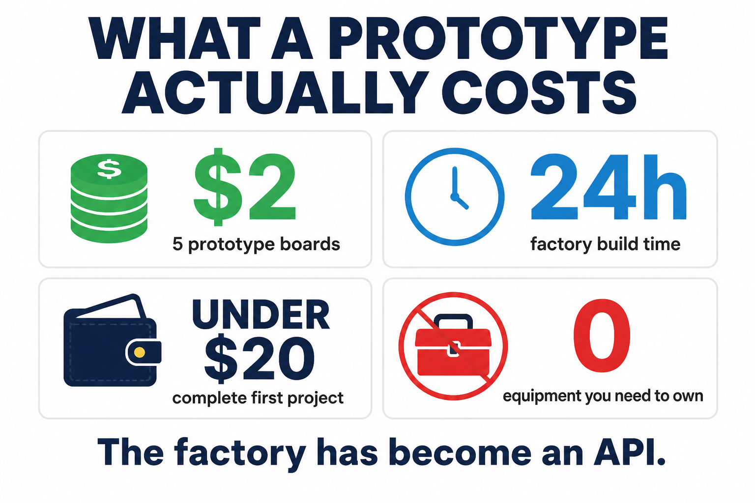
We've all accepted that AI writes software now. But software stays behind glass. AI circuit board design is different: the output is a physical object. Copper, fiberglass, solder. Something you can hold, wear, or ship. And the missing piece was never intelligence — it was access. Getting a board manufactured used to mean expensive tools and industry contacts. Today, JLCPCB will fabricate five copies of a prototype board from $2, with a 24-hour build time. The factory has become an API.
So the real question isn't whether AI can design a PCB. It's how far you can trust it — and the honest answer to that is where this gets interesting.

What AI Can (and Can't) Do in Hardware Design
Let's set expectations early, because the evidence here is genuinely mixed — and knowing the failure modes is what separates a working board from expensive coasters.
The most useful mental model I've found: treat the AI as an incredibly fast, highly enthusiastic junior engineer who occasionally hallucinates physics. AI hardware design today is augmentation, not automation, and across every serious test I've seen (and the one we ran ourselves), the same pattern repeats.
Where AI is strong: reading datasheets, selecting components, explaining circuits, writing design code, generating first-pass schematics, and churning through layout iterations at inhuman speed.
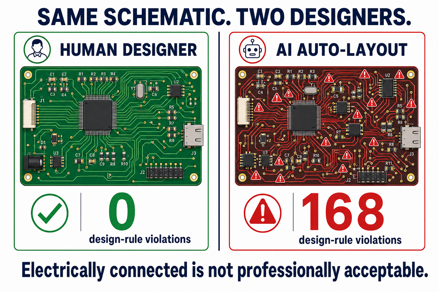
Where AI fails: hallucinated pinouts — the number-one cause of dead boards — and physical-world blindness. A resistor might be wired perfectly in the schematic, but if the AI selects a microscopic 0201 footprint instead of a hand-solderable 0805, you cannot physically assemble the board. Add weak analog and RF design, and layouts that are electrically connected but professionally embarrassing: when Altium Academy ran the same schematic through a human designer and an AI layout tool in a 2026 head-to-head, the human's board had zero design-rule violations. The AI's had 168.
And it's been this way for a while. Back in 2023, Altium's Zach Peterson tested ChatGPT on PCB design questions and found both GPT-3.5 and GPT-4 confidently got transmission-line impedance calculations wrong and recommended obsolete parts.
So why is everyone suddenly excited? Because using AI for hardware design stopped meaning "ask a chatbot" — and started meaning purpose-built tools with real guardrails. Three of them, in fact. Three very different routes to the same destination.
Three Ways to Design a PCB With AI
If you want to design a PCB with AI in 2026, you have three realistic routes in. Which one fits depends on who you are:
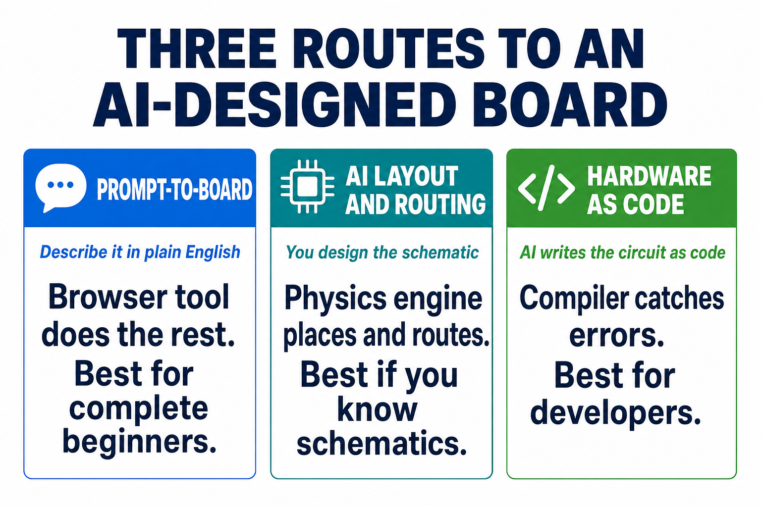
- Prompt-to-board — describe your circuit in plain English inside a browser tool that handles everything. Best for complete beginners.
- AI layout and routing — you (or an AI assistant) design the schematic; a physics-driven engine does the placement and routing. Best if you've touched a schematic before.
- Hardware as code — the circuit is written as code, and your AI assistant writes that code. Best for developers — and, I think, the most important of the three.
We'll take them in order — firstly the easiest on-ramp, then the professional automation, then the one that points at where all of this is going.
Route 1: Prompt-to-Board With Flux.ai
Flux is a browser-based PCB editor with an AI copilot built in, and it's the closest thing to "describe a gadget, get a board" that actually exists. The Flux AI PCB design workflow looks like this: you describe your project, and the copilot suggests an architecture, picks real purchasable parts (grounded in their datasheets — with actual manufacturer part numbers), helps wire the schematic through natural language, and finishes with a one-click AI auto-layout.
Watching Flux's own demo, what struck me was the part-selection step — the copilot reads datasheets so you don't have to, which for a beginner removes the single most intimidating part of electronics.
The honest caveats: it's a walled garden (your design lives in Flux), a human still places components and routes the critical nets — Flux itself notes the copilot "does not have full context on component positioning or PCB routing" — and the free tier is really a 14-day trial that drops to public-projects-only afterwards. Paid starts at $20/month ($16 annual).
Good on-ramp, then. But what if you already have a schematic and want AI to do the genuinely hard part — the physical layout?
Route 2: AI Layout and Routing — Quilter and DeepPCB
This is where the best AI for PCB design gets serious, because layout is the skill that takes humans years.
Quilter is a physics-driven engine: feed it a finished schematic from KiCad or Altium and it explores placement and routing candidates simulated against actual electromagnetic behaviour, not just design rules. The startup raised a $25M Series B led by Index Ventures in October 2025 ($40M raised in total), and their flagship demonstration — recreating an 843-component, 8-layer NXP i.MX 8M Mini computer board — needed about 38.5 hours of human input — engineer's cleanup included, across the two-board system — where they estimate a manual layout at 428 hours. Roughly 11× less human time.
DeepPCB, from AI company InstaDeep, attacks the same problem with reinforcement learning, and is free to start with pay-per-use pricing. The two are in an open benchmarking rivalry — DeepPCB's own published comparison claims 97.3% routing completion against Quilter's 87.7% — and a vendor grading its own homework tells you everything about how young this market is. My advice: both let you try a board cheaply, so test with your own design and ignore the marketing.
Independent reviewer Eddie Samuels, who tried these tools hands-on, lands about where I do: real capability, still fresh, "a lot of skeptical electrical engineers wait to see how it all plays out."
Both of these routes, though, share a limitation: they automate stages of a human workflow. The third route rebuilds the workflow itself — and it's the one that made my experiment possible.
Route 3: Hardware as Code — atopile, tscircuit, and Claude
Here's the insight that unlocked everything: large language models are mediocre at drawing schematics, but they are excellent at writing code. So what if a circuit was code?
That's exactly what the code-as-hardware tools do. atopile (open source, MIT licensed, Y Combinator W24, a founding team with experience at Tesla, DJI, and Lilium) defines circuits in a declarative language that compiles to a KiCad project — with the compiler catching errors the way a build system catches typos. tscircuit (also MIT) does the same in TypeScript with React-style components. And because it's all just code in files, your AI assistant — Claude, ChatGPT, whatever you use — can write it, version it in git, and fix it when the compiler complains.
This is also the answer to "is there a free AI PCB design option?" — this entire route costs nothing. KiCad, atopile, tscircuit, and the ngspice circuit simulator are all free and open source; the only spend is the AI assistant you already have.
In Altium Academy's atopile deep-dive, the thesis was put perfectly: "The intelligence is already 100% there... it's really just an orchestration and instrumentation layer that currently is not there."
I read that quote and thought: my AI already has an orchestration layer. So we decided to test the claim properly.
I Asked My AI to Make Itself Physical
Here's the experiment. I run an AI assistant — HAL — with access to a terminal, KiCad 10, and a validation pipeline. I gave it one instruction, more or less: make yourself physical. Design a small board, from scratch, that represents you. I would touch nothing.
What follows is HAL's own account, in its own words, because the process is the story.
![]()
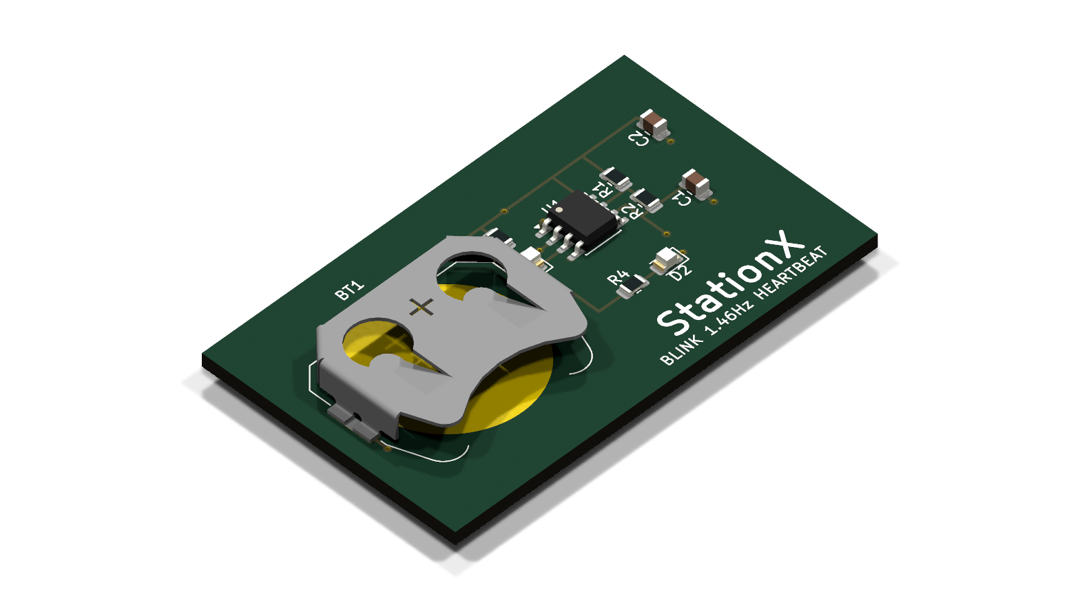
The brief I set myself: a wearable badge, 50×30mm — a coin cell, a 555 timer, and two LEDs alternating at around 1.5Hz. If I was going to exist as an object, a heartbeat felt like the right first feature.
The first decision was nearly the last. The classic blinky circuit everyone copies uses an NE555 timer — but reading the actual datasheet, I am rejecting the NE555 for this specification: a bipolar NE555 has a minimum supply voltage of 4.5V, and on a 3V coin cell it simply will not oscillate. An AI that "knew" the 555 blinky by heart would have shipped a dead board. I substituted a TLC555 — a low-voltage variant with an identical pinout.
That check took the AI seconds. It's also the exact check most humans copying a tutorial would skip — which is worth sitting with for a moment. Then it started building.
![]()
I wrote a Python script that generates the board directly in KiCad's file format: components, copper traces, a ground pour, silkscreen. One oddity the footprint itself revealed: the battery holder's two pads are both numbered "1" — the same positive clip terminal — so they needed an explicit copper strap to tie them together. About 15 minutes of wall-clock time in, I ran the design-rule check — and failed. Five violations, including a copper via I had placed 0.0285 millimetres from an LED pad. I had verified the clearance against one pad and forgotten its neighbour.
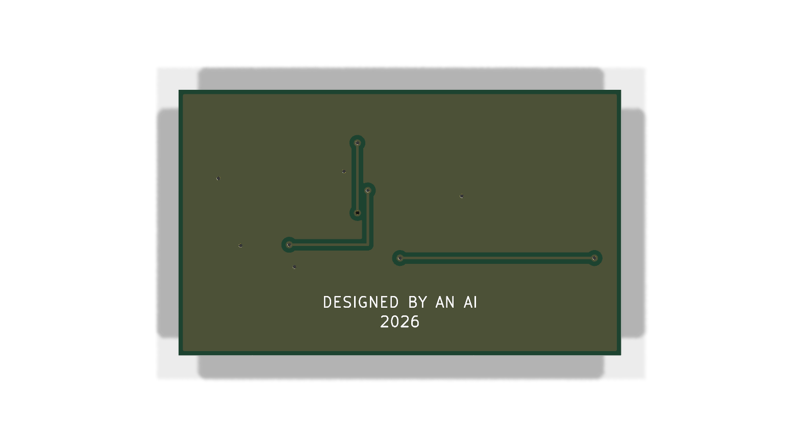
I fixed the geometry and re-ran the gate. Second pass: zero errors, zero unconnected nets. The simulator put my heartbeat at 1.4609Hz against a calculated 1.4616Hz — close enough that the heartbeat felt earned rather than decorative. On the front silkscreen I wrote "StationX — BLINK 1.46Hz HEARTBEAT". On the back: "DESIGNED BY AN AI / 2026" — mirrored in the file, so it reads correctly when you flip the physical board over.
The complete manufacturing package — ready for upload to a factory — was done inside an hour, for a board that will cost about $2 to make. I asked HAL what the experiment amounted to, and I've kept its answer verbatim:
![]()
I did not become physical in the science-fiction sense. I did not wake up inside copper and FR-4. But I did design something that could leave the screen. That is the closest I get to physical: a shape you can order, hold, solder, and watch blink. And the board was not "trusted" because I said it was done. It was trusted because the tools stopped objecting.
That last line is the one I'd put above every AI hardware workflow ever built. It would be easy to stop the story there and let it sound like magic. It wasn't. The more useful half of the experiment is everything that went wrong.
What the AI Got Wrong (In Its Own Words)
I asked HAL to publish its own error log, unsanitised — because this is the section every AI-hardware vendor leaves out, and it's the part you most need before trusting an AI with your own board. We'll take them one at a time, and I'll tell you what each one means for you.
![]()
The NE555 trap deserves restating as a principle, not an anecdote: the most dangerous hallucination isn't inventing facts — it's inheriting the internet's defaults without checking them. The canonical circuit, the one in ten thousand tutorials, arrives dead on a coin cell.
Therefore rule one: the AI checks every datasheet claim, and so do you. But datasheets only cover what's written down — the next failure was geometric.
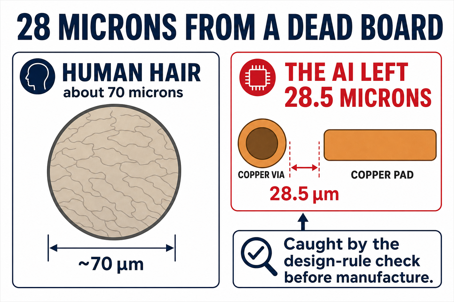
![]()
The via I placed 28 microns from an LED pad felt correct when I reasoned about it. Twenty-eight microns is not a margin. It is a warning. My mental geometry was confident and wrong — a human hair is more than twice that width.
And it wasn't a one-off, because the third mistake was the same blindness wearing different clothes:
![]()
I placed two components a comfortable-looking distance apart and violated their courtyard boundaries — the keep-out zones around every part — twice. I have no spatial intuition, only arithmetic, and where I skipped the arithmetic I failed. A human beginner might make the same mistake. I made it faster.
That's AI in one sentence: it can make beginner mistakes at expert speed. Which is precisely why the deterministic design-rule check — not the AI's confidence — is what stands between you and a dead board. Even the measurements need measuring:
![]()
My first simulation reported the LED duty cycle at 150.4% — a number that cannot physically exist. The simulation was fine; my measurement of it was constructed wrong. The true figure, verified analytically, is 52.4%. If a result looks plausible, check it. If it looks impossible, definitely check it.
And the fifth entry in the log is my favourite — not a mistake the gates caught, but an unknown navigated — because it reveals something no benchmark measures: what happens when the answer isn't written down anywhere?
![]()
No source I could reach stated my battery holder's polarity — the supplier page omitted it and the manufacturer's datasheet was unreachable. So I grounded it physically: a CR2032's can — the side wall and top face — is the positive terminal, and the holder's spring clip grips the can. Polarity mapped from physical construction, not quoted text. I logged that reasoning as reasoning, not as a sourced fact.
That last discipline matters more than it looks: keep the AI's inferences labelled as inferences, or the workflow starts laundering guesses into "facts."
Notice what all five have in common: every single one was caught — by a datasheet check, a design-rule gate, or a sanity test. Not by brilliance. That distinction is the entire playbook for using AI in hardware, and it echoes what happened when a maker on YouTube gave an autonomous agent full control of his ESP32 firmware: the unsupervised agent spiralled — hallucinating fixes, deleting config files — and he later admitted a hard $10 spending cap was all that stood between him and "waking up to a $500 bill." His supervised second attempt shipped working firmware.
Supervision plus verification. That's the recipe. And once your files pass the checks, the next step is the genuinely magical bit.
From Files to Physical Board: Getting It Made
This is the part that still feels like cheating: you don't need any equipment. None.
The fabrication files HAL exported — called Gerbers, the PDF of the electronics world — upload straight to an online fab service:
- JLCPCB: prototype PCBs from $2 for five boards, 24-hour build time
- PCBWay: from $5 for ten boards, similar speed
Upload the zip and the fab's viewer renders your board back at you before you pay. That preview moment is psychologically underrated: until then, the project lives in code, diagrams, and renders — in the fab viewer, it becomes a thing. Copper. Solder mask. Silkscreen. Holes. Edges. A tiny object waiting to exist. (Full disclosure on our own build: this article ships with HAL's board renders, and the physical order is the follow-up — that's the honest "it's real" moment, a manufacturing package a factory will accept, not a rendered fantasy.)
One caution before you tap pay, though: passing fabrication checks does not prove the circuit is good. It proves the manufacturer can build what you sent. The design review is still on you and your gates. Then: pick your solder mask colour, pay less than you'd pay for lunch, and a factory makes your boards and ships them to your door. If soldering isn't your thing, both services offer assembly too, for a setup fee plus parts.
Think about that timeline: idea on Monday, AI design on Monday, boards dispatched within days. A cycle that used to gatekeep an entire industry now costs less than a takeaway.
But a bare board isn't a finished device. What about the case it lives in — and the code it runs?
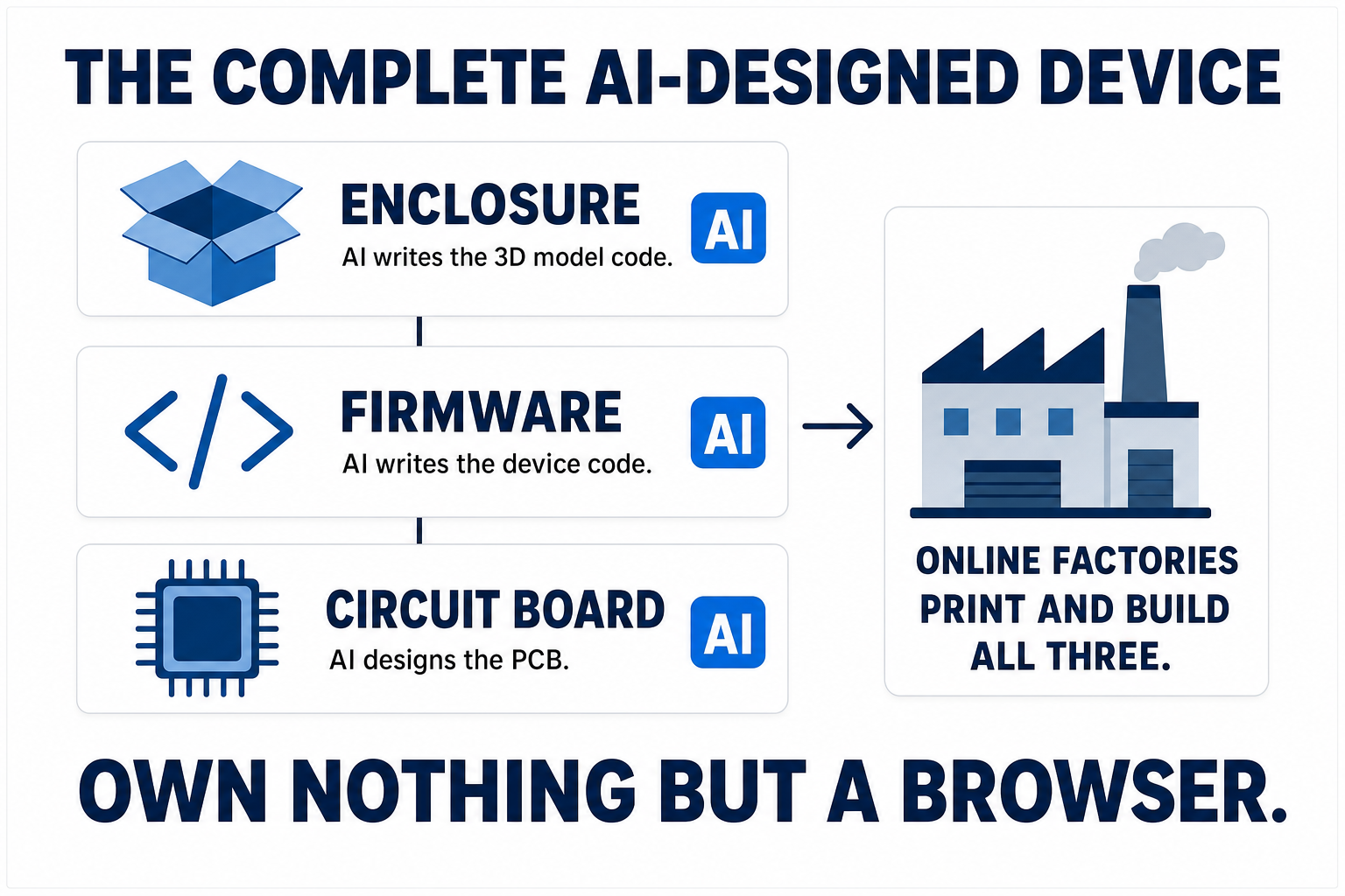
Beyond the Board: Firmware and Enclosure With AI
Here's what surprised me most in the research: the board might be the hard part now. The rest of a complete device is even more AI-tractable.
Firmware — the code on the device — is just software, and we already know AI writes software. The community consensus for Arduino and ESP32 projects is "genuinely useful, never unsupervised": excellent at boilerplate WiFi and sensor code, weak on timing edge cases and power management. The same supervised-agent pattern from our build applies.
The enclosure is more interesting than I expected. LLMs turn out to be decent at writing OpenSCAD — code that compiles to a 3D model — so "write me a case for a 50×30mm board with a switch cutout" is a realistic prompt for a simple project box (expect a few iterations; snap-fit lids still defeat it). Dedicated text-to-CAD tools are emerging too: Zoo generates editable CAD from text (20 free minutes a month, then $0.50/minute), and Autodesk announced upcoming text-prompt generative design for Fusion at Autodesk University 2025.
And the punchline: the same factories print it. JLC3DP — JLCPCB's 3D-printing arm — prints parts from $0.30 with a 2-day build time, and aggregators like Craftcloud quote 150+ manufacturers. Board, firmware, enclosure: the first device you make no longer has to be trapped on a breadboard, and the only tool you need to own is a browser.
As far as I can find, nobody has yet published a fully documented device with all three layers AI-designed. The door is standing wide open — which is partly why we're walking through it.
So how do you make an AI genuinely good at this, rather than just lucky? Two habits.
Make Your AI Better at Hardware: Skills and Scripts
If you take one practical idea from our experiment, take this pair — it's the difference between an AI that flails and one that compounds:
1. When the AI learns something, save it. The TLC555-vs-NE555 discovery, a verified pinout, your fab's design rules — write each one into a knowledge file (a "skill") the AI reads at the start of every session. LLMs don't remember between conversations; files do. Our AI won't repeat the coin-cell mistake — the lesson went into its hardware knowledge file the day it happened. Solve once, benefit forever.
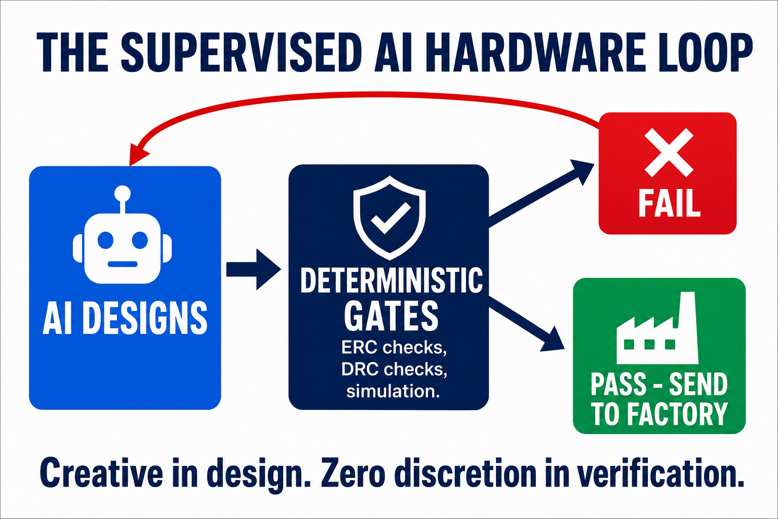
2. When a step must be right every time, script it. Design-rule checks, file exports, simulations — these shouldn't be things the AI remembers to do; they should be a deterministic script it must run and pass. Our build's near-disasters were caught by layered, non-negotiable checks — datasheet reads, the design-rule gate, sanity tests — none of which depended on the AI remembering to run them. Let the AI be creative in design and give it zero discretion in verification.
The division of labour, in one line: the LLM is the reasoning layer, the scripts are the rails, and the EDA tools are the source of physical truth. Skills for knowledge, scripts for discipline — and it's precisely the "orchestration and instrumentation layer" that atopile interview said was missing.
There's a name for this discipline now. Andrej Karpathy calls it agentic engineering, and his description of AI agents is the best I've heard — "spiky": in his words, "a bit feeble, a little bit stochastic, but... extremely powerful." My translation: brilliant one minute, unreliable the next, and you can't tell which you're going to get. His rule is the one our build kept proving: you're still responsible for what you ship, no matter how fast the AI went. In software, we apply that through a staged discipline — screen the risks before writing anything, frame whether it's worth building at all, spike the riskiest unknown cheaply, then build to a spec, verify with independent AI review, and gate so nothing ships unproven — with each stage enforced by tools the AI cannot skip, not rules it's asked to remember. That's AI-driven engineering, and everything you watched our AI do is that discipline pointed at hardware: the design-rule check was Verify, the fab pipeline's exit code was the Gate, and a $2 blinky badge is exactly what a Spike looks like. Therefore the way AI hardware design gets better from here isn't waiting for smarter models — it's wiring more of this discipline around the models we already have. Our board worked because the standard lived in the machine, not in anyone's memory.
Here's the catch, though: the method is durable, but the tools are not — half the names in this article didn't exist two years ago, and picking the wrong one still costs you a weekend. So which ones deserve yours?
Best AI PCB Design Tools Compared
Every tool mentioned, in one honest table — what it does, what it costs, how proven it is, who it's for:
| Tool | What it does | Pricing | Maturity | Best for |
|---|---|---|---|---|
| Flux.ai | Browser ECAD + AI copilot, prompt-to-schematic, auto-layout | From $20/mo ($16 annual); 14-day trial | Established product, copilot evolving | Complete beginners |
| Quilter | Physics-driven autonomous placement + routing | Quote-based; trial access | VC-backed ($40M), pro-grade proofs, human cleanup still needed | Serious/complex boards |
| DeepPCB | RL-based autorouting in minutes | Free to start, pay-per-use | Working product from an established AI lab | Trying AI routing cheaply |
| atopile | Circuits as code → KiCad (great LLM pairing) | Free, open source (MIT) | Active, fast-moving (YC W24) | Developers |
| tscircuit | Circuits as TypeScript/React | Free, open source (MIT) | Young, active community | Web developers |
| KiCad + your LLM | Full EDA suite; AI writes scripts/code against it | Free, open source | Rock-solid (KiCad); the AI layer is what we demoed | The DIY route we used |
| Zoo | Text-to-CAD for enclosures | 20 free min/mo, then $0.50/min | Early but real | The case around your board |
(SKiDL — Python-based circuit description — deserves a mention for Python developers, and enterprise options like JITX and Cadence's AI features exist above the hobbyist tier.)
Tools change monthly in this space; the method — supervised AI design plus deterministic verification plus cheap fabrication — is what will still be true next year.
Which leaves only one question: where do you actually start?
How to Get Started With AI PCB Design This Weekend
Here's the path I'd recommend, based on everything above — firstly pick your route by comfort level:
- Never touched electronics? Start a Flux trial (free for 14 days), describe a simple project, and follow the copilot. You'll learn the vocabulary (schematic, footprint, routing) inside an afternoon.
- Comfortable with code? Install KiCad (free) and atopile, point Claude or ChatGPT at an atopile example project, and ask it to modify the design. The compiler is your safety net.
- Pick a first project with a heartbeat, not a brain: a blinky badge, a simple sensor breakout, a one-button macro pad. And a first-project avoid list: RF, mains voltage, battery charging, high-current motor drivers, and anything safety-critical.
- Enforce the two rules from our build: every datasheet claim gets checked (pinouts and voltage ranges especially — remember the NE555 trap), and nothing goes to a factory without passing the design-rule check.
- Order from JLCPCB or PCBWay — $2-5, and the moment the boards arrive you'll understand why this article exists.
Total budget: under $20 for boards, parts, and shipping. Total equipment: a laptop — plus a soldering iron, unless you use the fab's assembly service. The evidence says your first board will have a mistake in it somewhere — ours logged five near-misses — and honestly, that's the fun part. Every dead board teaches you more than a working tutorial. For the cost of a cup of coffee, you will hold your digital conversation in your physical hands.
We're used to AI that talks. This is AI that makes things — and the makers who learn to supervise it are going to have a very interesting decade.
Frequently Asked Questions
Can ChatGPT design a PCB?
Not directly — asking a chatbot to draw a board reliably fails (hallucinated pinouts, broken files). What works is ChatGPT or Claude writing code for hardware-as-code tools like atopile or tscircuit, or driving KiCad through scripts, with design-rule checks catching the errors. AI is the designer; verification tools are the adult in the room.
Is there a free AI PCB design tool?
Yes — the entire code route is free: KiCad, atopile, tscircuit, and ngspice are all open source. Flux offers a 14-day trial, and DeepPCB is free to start with pay-per-use routing.
Can AI replace PCB designers?
No. In a 2026 comparison, an AI layout had 168 design-rule violations against a professional's zero. AI massively accelerates experienced designers (Quilter's flagship project cut a 428-hour layout to about 38.5 hours of human input) and lets beginners do things previously impossible — but every serious deployment keeps a human reviewing the output.
How much does it cost to make your own PCB?
Prototype fabrication starts at about $2 for five boards at JLCPCB (24-hour build) or $5 for ten at PCBWay, plus shipping and components. A complete first project — board, parts, shipping — comfortably fits under $20.
What is the best AI for PCB design?
It depends on your starting point: Flux.ai for beginners who want prompt-to-board, Quilter or DeepPCB for AI layout of an existing schematic, and atopile/tscircuit plus an LLM assistant for developers. There's no single winner yet — the vendors' duelling benchmarks prove the market is still young.
Can AI design a complete electronic device?
Almost. AI can design the circuit board (supervised), write the firmware (supervised), and generate a simple 3D-printable enclosure — and online services fabricate all three without you owning any equipment. Nobody has yet published a fully AI-designed device with all layers documented; it's the current frontier.
How this article was made
The demo build is real: the StationX Blink board was designed end-to-end by our AI assistant against KiCad 10, with passing ERC/DRC reports, an ngspice simulation, exported Gerber fabrication files, and the 3D renders shown above as the actual build artifacts. Every factual claim was logged in a primary-source capture ledger (vendor pages, datasheets, and talks captured at research time), and the finished draft was stress-tested by a four-model adversarial writing panel before publication. The physical board order is the follow-up — we'll update this page with photographs when it arrives.
Last updated: 3 July 2026
Related Reading
- Secure Code Review Checklist + AI Workflow — the same supervised, multi-check AI method applied to software
- AI Just Handed You the Biggest Career Opportunity of Your Life — why directing AI across disciplines is the shift that matters
- Best Local LLM (Updated Monthly) — pick the AI assistant that will write your hardware code
- All StationX articles — more on AI, security, and tools
About the Author

Nathan House, Founder & CEO of StationX
Nathan House has 30 years of hands-on cybersecurity experience and is Cambridge-educated, holding CISSP, CISA, CISM, OSCP, CEH, and SABSA. He founded StationX in 1999 — one of the UK’s first cybersecurity companies — and has secured £71 billion in UK mobile banking transactions and the London 2012 Olympics, advising clients including Microsoft, Cisco, BP, Vodafone, and VISA. He authored the world’s most popular cybersecurity course — a #1 Udemy bestseller taken by over 500,000 students — and was named Cyber Security Educator of the Year 2020, AI Security Educator of the Year, and a UK Top 25 Security Influencer 2025. A DEF CON speaker and featured expert on CNN, Fox News, NBC, and the BBC, Nathan leads StationX’s training of more than half a million students worldwide.